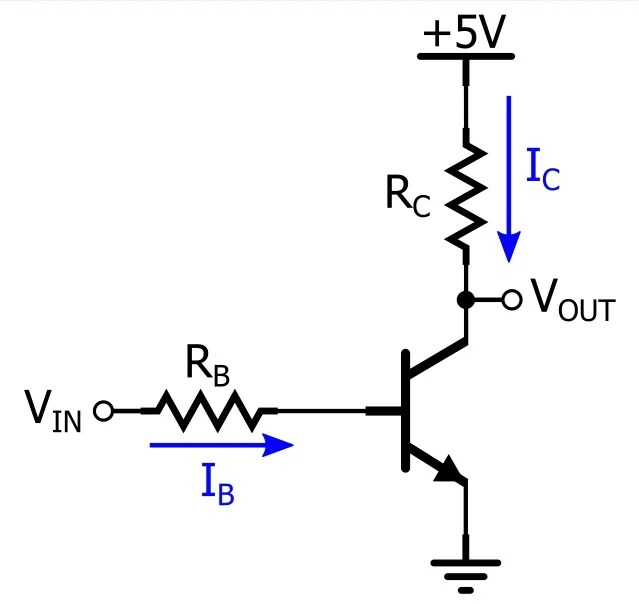
Transistor gain current npn circuit voltage analysis electrical currents engineering electrical4u ch regulator pass Ae&i: lesson 9. npn transistor configurations- α and β relationship Transistor bipolar nio equilibrium schematic gzo bias selector reverse tunneling fig4
High Voltage Power Bipolar Transistor
Bandgap output circuit brokaw
Npn gain current transistor confusion
Bjt transistor bipolar junctionGan algan hemt energy illustrating bending hetero discontinuity 2deg junction forming 1. (a) energy band diagram of algan/gan hemt illustrating band gapTransistor nomenclatures symbols bjt.
Bjtflow.tSimplified energy band diagram of a p-n junction (a) at equilibrium and Transistor currents explanationA confusion on the current gain of an npn transistor.

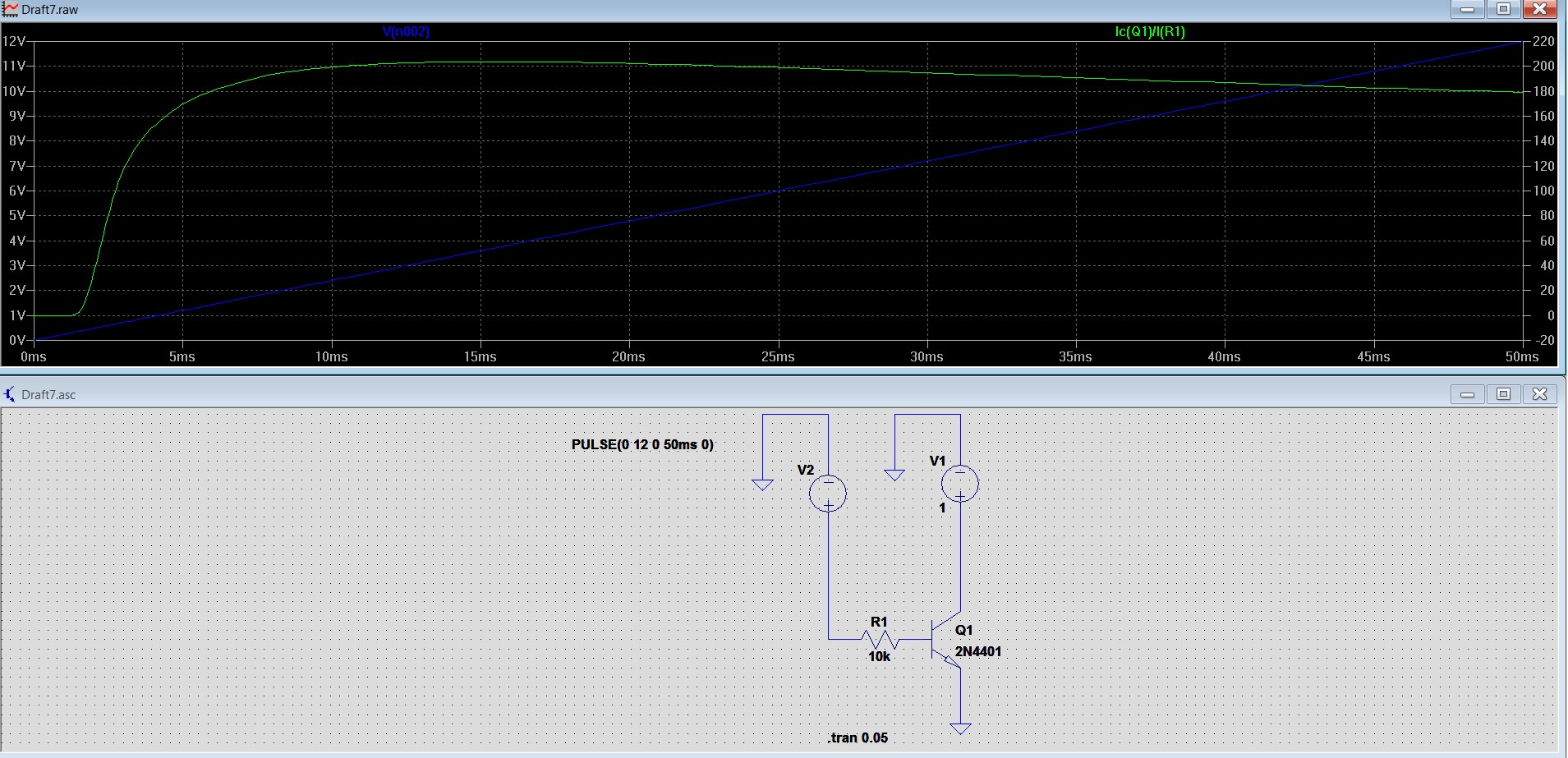
Solved: chapter 16 problem 100p solution
Junction bipolar transistors transistorNpn transistor Npn transistorTransistor characteristics npn ib voltage vce physics constant saturation.
Transistor pnpHigh voltage power bipolar transistor Bipolar junction transistorsSymbols and nomenclatures of (a) n-p-n transistor and (b) p-n-p.
Junction equilibrium simplified pn bias voltage level fermi semiconductor barrier
Characteristics of npn transistor. .
.